Driven by AI, the evolution of smart machines has been remarkable, learning and deciding autonomously. In pursuit of groundbreaking advancements, innovators leverage Moore’s Law and 3D-stacked CMOS technology to elevate machine capabilities to unprecedented heights.
Working on top of Moore’s Law, the three-tier chip design flings computing capability sky high. A big letup in digital brainpower comes nestled within these chip layers. Machines can now think faster and hold even more facts, making it seem like they are almost beyond human wisdom.
Unveiling the Foundations
By beginning with a discussion of how 3D chips are layered, we need to look back at the base rule of how our modern gadgets keep getting better Moore’s Law. The idea came from a man named Gordon Moore in ’65, saying that small parts called transistors would grow in number really fast, about two times in every pair of years. As years passed by, this simple rule of rise was followed, setting a steady path for people making computer chips to push hard for making things a tiny cow and work smooth.
Gadgets today are smarter thanks to Moore’s Law. The cleverness of these chips has soared because more parts can fit in. Since this insight by Moore, which sounds like a lowering footstep toward future dreams, comb-makers have chased after the creeping shadow of making Widow everyday stuff ramp-up round quick and pennywise.
The Limitations of Traditional Scaling Approaches
Unquestionably, the way chips were made had to change. More and more little parts were not fitting well together. Because the parts got so tiny and heat was a big problem, new special ways had to be created for making these chips.
Chips were jammed with many tiny switches, and it was tough; now extra tiny parts can’t help much more. Packed on one chip, traditional styles stumbled over this roadblock, proving counterparts could be smarter. Undeniably urged by dire needs, ingenuity brewed – feeding tech’s hunger for the tinier gears Moore’s Law guessed would continue to sprout.
Enter 3D-Stacked CMOS Technology
Making electronic chips better is tricky. People got incredibly clever, though. In a surprising twist, layers upon layers of small electronic parts got stacked up high, one over the other, inside the tiny square brains of our gadgets, which started to take on a brand-new shape.
It’s not like the flat chips everyone knew before. The heat that builds up inside these tiny brains is being looked after better than ever. Given that, we might soon see computer brains in the shape of miniature skyscrapers zigzag their way to cooler operation and smarter performance.
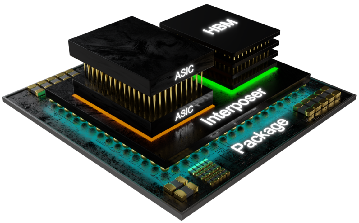
How 3D-Stacked CMOS Works
At the core of 3D-stacked CMOS technology is the vertical stacking of transistor layers. Each layer, consisting of transistors and interconnects, is carefully designed to complement the layers above and below. The vertical integration allows for shorter interconnects, reducing signal delays and enhancing overall performance. This architectural innovation breathes new life into Moore’s Law, enabling a more efficient use of resources and a sustained trajectory of computational advancement. Moreover, AI-Enhanced Accessibility in Fusion Energy further amplifies the potential of this technology, promising groundbreaking strides in energy research and accessibility.
The Impact on Computational Density and Performance
By placing tiny switches on top of each other on a small chip, lots of them can fit into a very little spot. When we do this, a chip without taking up more room gets really strong. This way to make chips better is special and changes a lot of things.
Because people found this way to put so many switches into such a snug space, they didn’t have to make the tiny pieces tinier. Doing that had been pretty tricky before. By stacking them up this way, some hard puzzle pieces have been moved out of the puzzle, thereby making the game a bit easier to play.
A Crucial Advantage
Beyond raw computational power, the adoption of 3D-stacked CMOS technology brings about a notable improvement in energy efficiency. The reduced signal distances between vertically stacked layers lead to lower power consumption, addressing a critical concern in the development of energy-efficient computing solutions. As the demand for sustainable and eco-friendly technologies grows, the energy-efficient nature of 3D-stacked CMOS becomes a key enabler for the future of AI and other high-performance computing applications.
Challenges and Future Prospects
While 3D-stacked CMOS technology holds immense promise, it is not without its challenges. The intricacies of manufacturing these vertically integrated chips require precision and technological advancements. Additionally, questions regarding cost-effectiveness and widespread adoption linger. As the industry grapples with these challenges, researchers and engineers are tirelessly working to refine the technology, paving the way for its seamless integration into mainstream semiconductor production.
Elevating Moore’s Law with 3D-Stacked CMOS Technology
The trajectory of AI and high-performance computing is poised for a transformative leap forward, and 3D-stacked CMOS technology stands at the forefront of this revolution. By elevating Moore’s Law to new heights, this innovative approach not only addresses the limitations of traditional scaling but propels us into an era of unprecedented computational power, energy efficiency, and technological possibilities. As the industry continues to embrace and refine 3D-stacked CMOS, the synergy between AI and semiconductor technology promises a future where the boundaries of computational capability are continually pushed, opening doors to uncharted realms of innovation and discovery.